So you have your z8f0811 device from the ‘90s and you’ve misplaced the source code; what do you do? There is a simple method and a more complicated method if Read Protect was enabled during flash programming, using a Raspberry Pi as a flash programmer.
Using Debug PIN
The z8f0811 has debug pin, which controls the OCD interface (which has the descriptive name “On-Chip Debugger”. One of the commands is Read Program Memory (0BH). Since this is a one-pin interface, I connected an arduino and wrote the following program.
1 | int pin = 3; |
Then I connected my logic analyser to see what came back. It did send 0x2000 bytes – all of them are 0xff though! Turns out that the z8f0811 has a feature called Rom Protect (RP).
Bypass Possible?
While searching for a solution for this, I came across this Z8F04xx,08xx Errata, which says:
The Read Protect (RP) Option Bit does not prevent Flash access when bypassing the Flash Controller as described in ZiLOG Application Note AN0017 entitled Third Party Flash Programming Support of the Z8 Encore!® MCU.
User code cannot be read through the On-Chip Debugger when read protect is enabled. User code can only be read out when bypassing the Flash Controller.
Work-Around:
None
Now that is interesting! So here we have that document: Third Party Flash Programming Support for the Z8 Encore. It describes a method for reading and writing the flash memory of the z8f0811 directly on the pins.
Implementation (hardware)
The first hurdle was to remove the z8f0811 from the board. I tried using a regular soldering iron, and found it impossible. I ended up buying a hot air soldering station, which is much better.
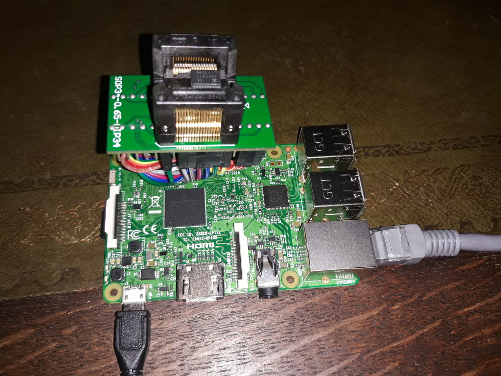
Having removed it, I then tried various ways of attaching things. The distance between the pins is 0.65mm so it’s very hard to work with. That was until I found this IC Test Burn-In Socket Adapter IC SSOP34 SOP34 to DIP34 OTS-34-0.65-01. Using this it was a breeze.
My arduino did not have enough gpio pins, and I suspected that it couldn’t generate a clock signal (PWM) either. So I used a Raspberry Pi for this.
According to the documentation, the lowest clock rate the z8f0811 supports is 32KHz. So on the Raspberry Pi I use pwm to generate that clock; then I connect that to Xin on the z8f0811, and also to another gpio pin on the Raspberry Pi so I can wait for the rising edge.
Most other pins need connecting: debug for setting flash bypass, reset for resetting the device after the pwm clock is set up, and all of port A, B, C pins (11 pins).
Implementation (software)
We’ll need to bit-bang various pins so even at 32KHz, we need to be very careful about being timely. The only way to do this in Linux is by writing a kernel driver, and holding a spinlock (to avoid interrupts).
Kernel driver and a Raspberry Pi config.
This is built against kernel 4.13-rc4 (simply because I was using that kernel version for testing RC core changes on the Raspberry Pi, and I knew that that version worked). This is using Fedora 26 (armhf).
After booting the kernel, you can copy the flash memory using:
1 | dd if=/dev/zdumper of=z8f0811.bin bs=8192 count=1 |
Finally
Presumably suspect the other z8f08xx and z8f04xx devices will work fine too; they need the same pins connected. I have not tested this.
I realise this device is a microcontroller and not a microprocessor, but I can’t help but dislike the instruction set. Why are there so many addressing modes for 4kb of ram/registers? The disassembly is painful to read and write, as the same register can be access in many different ways.